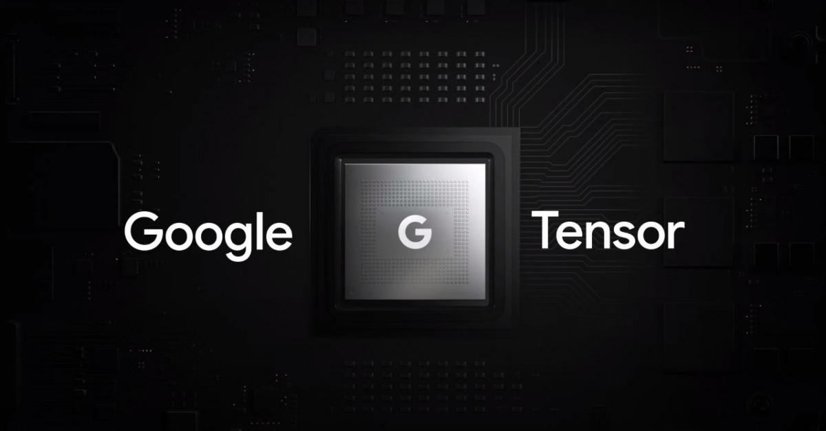
Google Tensor G2 is fabbed on 5nm process as per company spokesperson
Google unveiled the Pixel 7 series last week but did not share detailed specs about the new Tensor G2 chipset. Earlier rumors pointed to a 4nm manufacturing process but as it turns out the new SoC is based on a 5nm process as a Google spokesperson confirmed to Android Authority.
We don’t get official confirmation if Tensor G2 is built on Samsung’s 5LPE process like the Tensor G1 or the newer 5LPP process. The confirmed specs for the Tensor G2 CPU includes 2x Cortex-X1 cores, 2x A78 and 4x A55 cores along with updates in clock speed while the GPU is a Mali-G710 MC10.
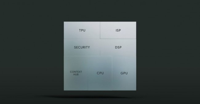
Google Tensor G2 chipset architecture
While a 5nm chipset may not deliver the same power efficiency as a 4nm chipset, Google’s new Tensor Processing Unit (TPU) is marketed as offering improved power efficiency as well as handling camera and machine learning tasks 60% faster than the Tensor G1's TPU.
Related


Reader comments
- maniac
- 13 Oct 2022
- rrH
Its not a Midrange...the performance is really smooth,the scores are almost on par with s22's
- Nick Tegrataker
- 13 Oct 2022
- Xpf
So Tensor G2 really is more of a midrange SoC by today's standard. I only use high-end smartphones so I guess it's an automatic no from me.
- Anonymous
- 13 Oct 2022
- 70d
The point of the embargo is that they don't want some reviewers to have advantages. Some reviewers get products for review faster than other reviewers. Another reason is that with the embargo, the reviewers won't feel to need to rush and pu...


 Samsung
 Xiaomi
 Samsung
 Sony
Sony Xiaomi