Samsung has finished the development of next-gen 5nm EUV node
Samsung just announced that it has successfully completed the development of its next-gen 5nm EUV manufacturing process and it's ready to ship samples.
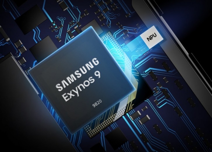
Samsung claims that the 5nm node boasts 25% better logic area efficiency with 20% lower power consumption or around 10% higher performance for the same power draw. The 5nm node is based on the same EUV lithography process and it will be manufactured at Samsung's Hwaseong foundry.
The foundry, by the way, will expand its capacity by the second half of this year and ramp-up production in early 2020.
It's still too early to tell but given the roadmap of the 7nm process, the company will most probably start mass producing the new chips in 2020, just in time for the next Galaxy S lineup.
In addition to the 5nm, Samsung is also working on a 6nm EUV-based chips in collaboration with some of its customers. Our best guess is that it's a lower cost process than the 5nm and will be suitable for mid-range to upper mid-range products.
Related


Reader comments
- Walter C. Dornez
- 19 Apr 2019
- qig
It's possible, but your original comment implied that you believed Huawei would go 3nm. I simply meant to correct that expectation
- AnonD-731363
- 18 Apr 2019
- SH3
Which is 2 years. THe 2nm will come in another 2 years and 1nm in another 2 years which wil be 6 years tottal and i said 5-7 up to 10.
- Walter C. Dornez
- 18 Apr 2019
- qig
I agree, but I doubt 3nm can come that fast. The jumps recently are because the chips still have enough space for the transistor and such, but 3nm might take at least until 2021 to get.


 Xiaomi
 Samsung
 Samsung
 Nothing
 OnePlus