Samsung begins production of first-gen 3nm chips
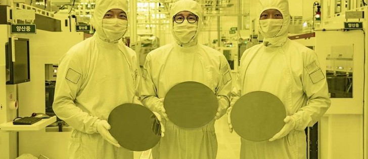
Samsung Foundry announced that it's beginning mass production of its first-generation chips on the 3nm node. It's based on the new GAA (Gate-All-Around) transistor architecture, which is the next step after FinFET.
Compared to 5nm, Samsung's first-gen 3nm chips can provide up to 23% better performance, up to 45% reduced power consumption, and a 16% reduction in surface area.
Samsung's second-gen 3nm node will be even more impressive - compared to 5nm, Samsung touts that it will achieve a 50% reduction in power consumption, up to 30% improvement in performance, and a 35% reduction of area.
Samsung is now ahead of TSMC, which is expected to begin mass production of 3nm chips in the second half of the year.
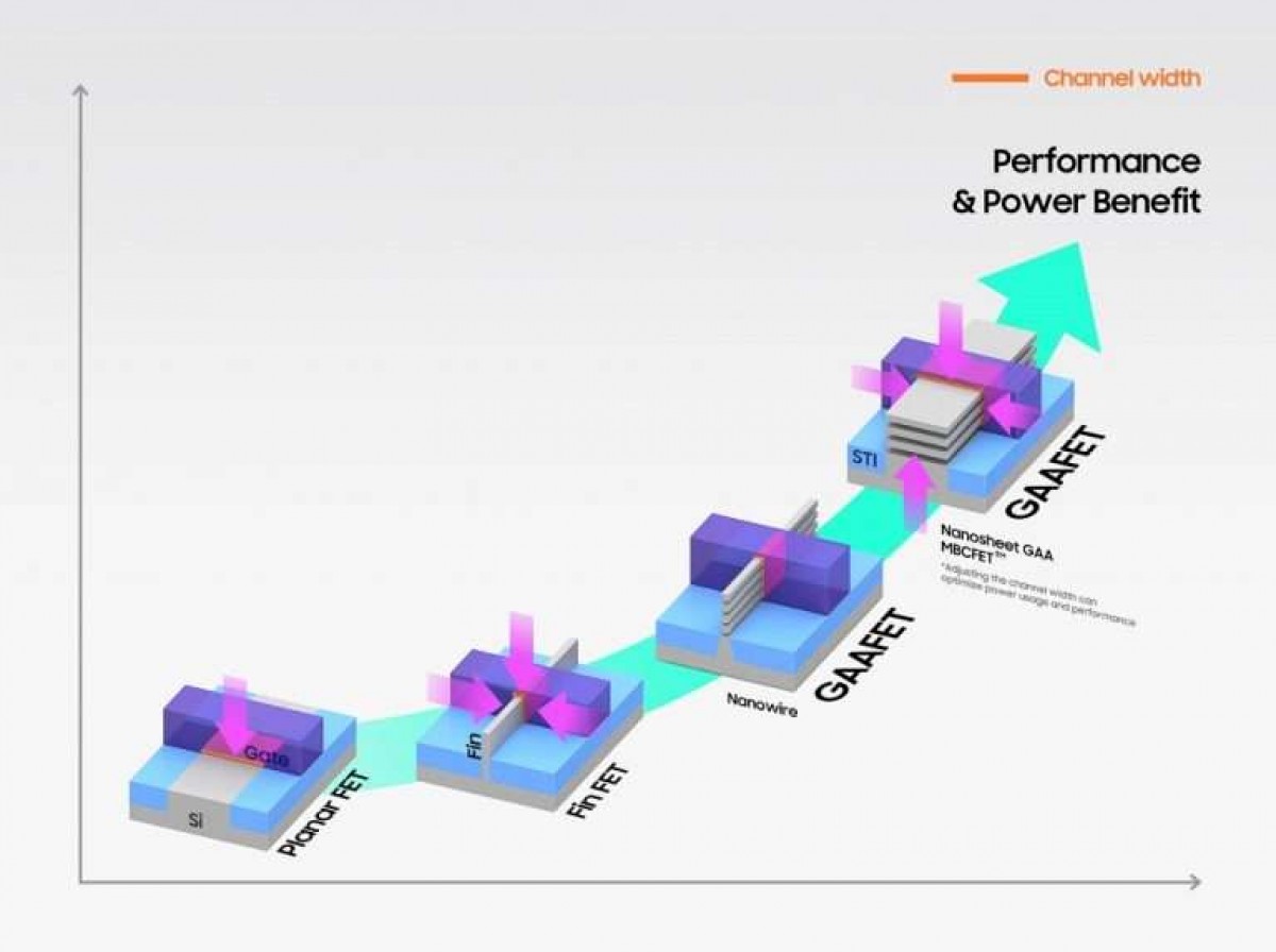
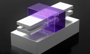
Gate-All-Around (GAA) transistor design allows the foundry to shrink transistors, without hurting their ability to carry current. The GAAFET design used in the 3nm node is the MBCFET flavor shown in the image below.
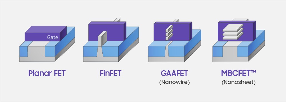 The evolution of silicon transistors
Related


Reader comments
- S Yu
- 03 Jul 2022
- vU9
TSMC's 5nm volume is decent enough for them to be taking GPU orders, what you're missing is that TSMC's nodes are far better so have far higher demand accordingly. Samsung's 1st gen 3nm...if they're lucky they could get it to...
- AnonD-762416
- 02 Jul 2022
- Sec
Projection, projection, projection. Lie as much as you like, reality does not care.
- Ishit Gandhi
- 02 Jul 2022
- 7k4
What a heat Samsung is bringing in the processor industry....


 Sony
Sony Samsung
 Xiaomi
 Apple
Apple Apple
Apple