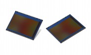
Samsung unveils 14nm FinFET technology for 144MP image sensors

Usually, when we talk about nanometers it’s about the latest chipset. However, a Samsung team at the IEDM 2019 conference presented a technology promising 144MP image sensors based around 14nm FinFET process.
The main challenge is that image sensors need to work at a relatively high voltage (2V and up) and all chipset designers aim for the lowest possible voltage (as that reduces power consumption and heat).
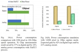
According to Samsung’s researchers, the 14nm FinFET technology will allow for a 42% reduction in power consumption in a 144MP sensor while capturing images at 10fps. For a 12MP readout at 30-120fps (i.e. recording video), the power savings can be up to 37%.

Samsung details plans for image sensors built on a 14nm FinFET process
Note that this announcement has nothing to do with pixel size – instead, the 14nm refers to the transistors that amplify the signal coming from the pixels along with other analog and digital processing hardware that’s on the image sensor.
Related


Reader comments
- Anonymous
- 18 Dec 2019
- I8m
Who else? Maybe the only person you were talking to that the subject matter even refered to in what I said???
- AnonD-731363
- 18 Dec 2019
- SH3
This is interesting but costly right now.


 Samsung
 Xiaomi
 Nothing
 Samsung
 Samsung